ADCLK846BCPZ-REEL7
Takt-Fanout-Puffer, 6 Ausgänge, 1.71 bis 1.89V, 1.2GHz, -40 bis 85°C, LFCSP-EP-24

Ihr Bedarf geht darüber hinaus?
| Menge | Preis (ohne MwSt.) |
|---|---|
| 1+ | 12,990 € |
| 10+ | 9,000 € |
| 25+ | 7,960 € |
| 100+ | 6,780 € |
| 250+ | 6,600 € |
| 500+ | 6,470 € |
Produktspezifikationen
Produktbeschreibung
ADCLK846 is a LVDS/CMOS, fan-out buffer optimized for low jitter and low power operation. Possible configurations range from 6 LVDS to 12 CMOS outputs, including combinations of LVDS and CMOS outputs. Two control lines are used to determine whether fixed blocks of outputs are LVDS or CMOS outputs. The clock input accepts various types of single-ended and differential logic levels including LVPECL, LVDS, HSTL, CML, and CMOS. It is widely used in application such as low jitter clock distribution, clock and data signal restoration, level translation, wireless communications, wired communications, medical and industrial imaging, ATE and high performance instrumentation etc.
- Upto 6 LVDS (1.2GHz) or 12 CMOS (250MHz) outputs
- Integrated random jitter (LVDS) is 54fs rms typical at (BW = 12KHz to 20MHz, CLK = 1000MHz)
- Broadband random jitter (CMOS) is 100fs rms typical at (input slew = 2V/ns)
- Propagation delay (LVDS) is 2ns typical at (VICM = VREF, VID = 0.5V)
- Output rise/fall time (LVDS) is 135ps typical
- Output-to-output skew (LVDS) is 65ps typical
- Sleep mode, pin-programmable control
- Power supply is 1.8V typical
- Operating temperature is -40°C to +85°C
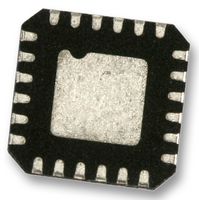
- Package style is 24-lead LFCSP
Hinweise
ADI products are only authorized (and sold) for use by the customer and are not to be resold or otherwise passed on to any third party
Technische Spezifikationen
Fanout-Takt-Puffer
6Ausgänge
1.89V
24Pin(s)
85°C
-
No SVHC (21-Jan-2025)
1.2GHz
1.71V
LFCSP-EP
-40°C
-
MSL 3 - 168 Stunden
Technische Dokumente (2)
Zugehörige Produkte
1 Produkt(e) gefunden
Gesetzgebung und Umweltschutz
Land, in dem der letzte Fertigungsprozeß ausgeführt wurde.Herkunftsland:Philippines
Land, in dem der letzte Fertigungsprozeß ausgeführt wurde.
RoHS
RoHS
Produkt-Konformitätszertifikat